


Univerza v Novi Gorici
LQO:
The Laboratory of Quantum Optics is equipped with an ultra-high-speed Titanium:Sapphire (Ti: Sa) laser system, an optical parametric amplifier, and a beam line for high harmonics generation in gas (HHG). Using this equipment, LQO can generate femtosecond (10-15 fs) laser pulses ranging from infrared (2600 nm) to extreme ultraviolet light (16 nm). These pulses are used in experiments on time separable photoemissions for studying electronic and structural properties of materials outside the thermodynamic balance. Two experimental chambers are used to achieve this: one is fitted with a VG-Scienta R3000 conventional hemispherical electron analyzer and the other with an ARTOF 10K spectrometer enabling capturing time- and angle-separated electron specters. One of the chambers has a classic source of X-ray lighting which, combined with an electronic analyzer, and is used in experiments on static, high-resolution X-ray photoemission. The latter allows a physical and chemical analysis of materials with high energy and angular resolution. The list of equipment is available at: http://www.ung.si/en/research/laboratory-of-quantum-optics/Equipment/.
LOMP: The Laboratory of Organic Matter Physics is equipped with a system for preparation and characterization of thin layers carried out in a controlled N₂ atmosphere with no oxygen or water. Thin layers are either vapor deposed by heating or using an electronic canon inside a high-vacuum chamber or applied from a solution. Characterization of thin non-conductive, conductive and semi conductive layers is designed to study morphological and opto-electronic properties. Opto-electronic properties are studied using the ETO method for photo-generated charge carriers (ETO photoconductivity). This is done using a variable wavelength 3ns pulse laser in the 210 nm-2300 nm range and at temperatures ranging from 12K to 300K. The resulting photo-generated pulses of electric current are measured with measuring tips (4 GHz), high-speed current amplifiers (2 GHz), and a digital osciloscope (2.5 GHz). The system’s grade AAA solar simulator also allows for characterization of thin film transistors and solar cells. The system can be adapted to perform measurements while epitaxially preparing an active layer in a high vacuum. Further details are available at http://www-lfos.ung.si/list-of-equipment.
LMR: The Materials Research Laboratory is equipped with a scanning electron microscope with field emission (FE-SEM) JEOL JSM-7100F. The wide energy range of the e-beam (0.1 – 30 keV) allows the monitoring of a wide variety of samples, from polymers to inorganic materials. The electric current per sample is between <1 nA to 300 nA, which allows capturing high definition images (HD <2 nm, at 30 keV) as well as using sensitive microanalytical techniques. The microscope is equipped with a secondary electron detector, a backscattered electron detector and a “through the lens” (TTL) detector with an energy filter.
From the analytic techniques point of view, SEM is equipped with an energy dispersion spectrometer – EDX (X-MAX80, Oxford Instruments), which enables the implementation of high resolution spectroscopic analysis (127 eV resolution at the Mn Kα line) for the characterization of the sample composition and mapping of the elements. In addition, SEM is also connected to a cathodoluminescent detector (MonoCL4, Gatan), which enables spectroscopic measurements and emission mapping within the visible spectrum (300-800 nm) due to the excitation of the sample with an electron beam. The laboratory is also equipped with sample preparation devices, eg. a diamond saw, a polishing machine, a precision etching and coating machine (PECS, Gatan), and a precision ion polishing machine with an Ar beam (JEOL).
Further details available at: http://www.ung.si/en/research/materials-research-laboratory/equipment/
![]()
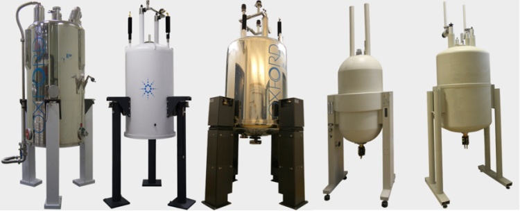
The National Center for High Resolution NMR spectroscopy
The full list of equipment is available at: http://www.slonmr.si/sub_sites/instruments.php.
The National Institute of Chemistry (NIC)’s Center for NMR spectroscopy (SLONMR) has five instruments, the quality of which is crucial for the implementation of the most advanced research and thus providing the high quality research and publications in the international arena. The 800 and 600 MHz NMR instruments are equipped with a state–of-the-art cold probe and use their high resolution and sensitivity to enable a study of the 3D structure and dynamic of the complex systems with a high molecular weight, such as proteins, nucleic acids and polymers in solution. The increased sensitivity allows for measuring samples of smaller systems with a lower concentration, as well as samples with less stability. The second 600 MHz NMR instrument is used to study a variety of solid samples, from new active pharmaceutical ingredients to different materials of inorganic and organic origin. The two 300 MHz instrument are essential for monitoring the synthesis and the analytics in the pharmaceutical, chemical, food and other industries.

Technische Universtät Graz
Synchrotron:
DXRL: http://www.ceric-eric.eu/index.php?n=PartnerFacilities.Elet6
SAXS: http://www.elettra.eu/elettra-beamlines/saxs.html
Laboratory: SAXS
http://www.ceric-eric.eu/index.php?n=Users.Facilities
Polymer Competence Center Leoben GmbH
PCCL has a great amount of equipment for measuring and testing materials, and conducting scientific research and technical tests in the field of polymers.
Mechanical material testing devices, such as a servo hydraulic apparatus (MTS 858) for material characterization under different conditions (tension, compression and bending) and with different load measurement methods (static, dynamic, cyclic). The Bose Electroforce 3200 machine is used for the dynamic-mechanical tests with the cooler unit (-60 °C to 300 °C), and for determining the material creep. Soon, a nano indentation device will be made available for a more precise determining mechanical tests of thin films. Several DMA devices are available for conducting thermomechanical tests (eg. a Perkin Elmer DMA 8000). Measuring thermal conductivity of polymers/composites is carried out on a Guarded Heat Flow Meter (DTC 300; TA Instruments), and the thin-film samples on a Laser-Flash device (Netzsch).
Sample surface test can be done on a rotary tribometer (Phoenix) and a micro-tribometer (Bruker UMT-2). The surface energy is determined with the help of a contact angle measuring device – a goniometer (Krüss DSA 100) and a tensiometerom (Krüss K100) for determining particle and fibre surface energy. The activation for the surface treatment of polymeric surfaces can be carried out with a Corona (Ahlbrandt) machine, a plasma reactor (Oxford Instruments) and under different UV light sources.
PCCL also owns an extensive selection of optical devices for showing surfaces of materials, which includes a 3D Mapsystem Leica DCM 8, which can measure interferometry, confocal microscopy and focus-varied microscopy (vertical resolution of 0.1 nm and a horizontal resolution of 140 nm), an Infinite Focus system (Alicona) as well as optical microscopes. The selection of surface research equipment is completed by an atomic forces microscope (AFM).
PCCL uses various spectroscopic methods for physico-chemical characterizations of polymers, such as a FTIR and ATR-FTIR spectrometer (Perkin-Elmer), a Raman microscope (Jobin.Yvon), a low-field NMR spectrometer (Bruker Minispec), and a UV/VIS and fluorescence spectrometer. Molecular characterization of polymers and molecules of low molecular weight can be processed with an HPLC-MS system, gel permeation chromatography (GPC) and gas chromatography (GC-MS) by pyrolysis, inter alia.
Conditioning of samples and researching longterm polymer behaviour (such as foil) in conditions involving UV light, heat and humidity can be carried out using several aging devices (including Xenotest, Suntester by Fa. Atlas) and climatic chambers.
![]()
Silicon Austria Labs (SAL)
General information on SAL’s R&D facilities is available on their official website: https://silicon-austria-labs.
The RETINA project will mainly be using Raman spectroscopy to process material characterization. As per the application, SAL will invest in the Anti-Stokes upgrade of the existing Raman system, which will be particularly useful for type 2 pioneering operations. Their main focus will be the characterization of internal tensions in silicon used in solar cells, etc. They will also provide spectroscopic research for type 1 pioneering operations.
Renishaw and Via Reflex confocal Raman microscope
General description: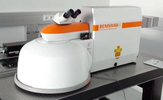
The Raman microscope enables Raman spectroscopic analysis of both macroscopic and microscopic samples up to the submicron resolution level. Its wide range of applications include determining the molecular composition of samples, measuring load and voltage in semiconductor materials, etc. The instrument allows 2D and 3D mapping, bulk sample analysis using an external hand or optical fibers, and the analysis of samples too large for the sampling chamber.
Key features:
- Spectral range: <100 – 4000 cm-1 at a spectral resolution of < 1 cm-1
- Three excitation lasers: 532 nm | 633 nm | 785 nm
- Three diffraction gratings: 1200 | 1800 | 2400 l / mm for a wide spectral coverage or high resolution
- Front lenses: 5 | 10 | 20 | 50 | 100x
- A motorized 3D table with sub-micrometer precision
- Automatic 2D/3D imaging
- Equipment for analyzing bulk or liquid samples
- Equipment for analyzing large samples outside the sampling chamber
- High-quality data evaluation using the latest version of the WiRe® software
The project also includes the use of the equipment listed below.
Bruker LUMOS FTIR microscope
General description: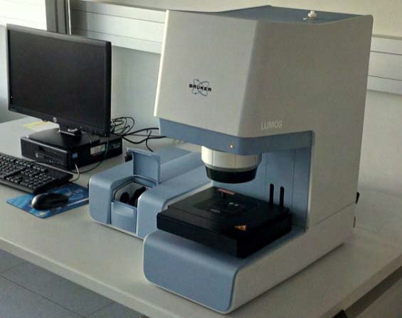
LUMOS is a fully automated, self-contained, medium wavelength, infrared microscope. It allows the analysis of macrometer and micrometer samples using the transmission, reflection or attenuated reflection (ATR) methods. Its use involves identification of particles, contaminations and the surface layers, and analyzing the chemical composition of complex samples. The instrument enables point analysis and detailed 2D mapping. It is also equipped with a MACRO unit with different add-ons that enable the analysis of large samples.
Key features:
- Spectral range: 650 – 4000 cm-1 at a spectral resolution of 2 cm-1
- Measuring options: transmission | reflection | attenuated reflection ATR (Ge crystal)
- A powered, high-precision 3D table with a 75 x 50 mm2 work area for samples of up to 40 mm of height
- 8 x lens with a VIS polarization option
- Automatic 2D imaging
- Equipment for the analysis of bulk samples: transmission, diffuse reflection
- A large data base for the spectral identification of unknown substances
Polytec Micro System Analyser MSA-500-TPM
General description:
The Micro Systems Analyzer is a measuring tool for the analysis and visualization of planar and non-planar structural vibrations and the surface topography of micro structures such as MEMS. The MSA Instrument is equipped with a microscope, laser vibrometry, strobe videomicroscopy and white light interferometry and thus combines technologies that reveal the real microstructural responses and topography.
Key features:
- Interferometry with white light (3D topography)
- Z-resolution: nm range
- Lateral resolution: up to 500 nm (depending on the magnification)
- Laser doppler vibrometry (non-planar vibrometry)
- Frequency: 0-20 MHz
- Resolution: pm area (depending on the magnification)
- Maximum speed: ± 10 m/s
- Stroboscopic video microscopy (planar vibrometry)
- Frequency: 0-1 MHz
- Resolution: nm range (depending on the magnification)
The Bruker Dektak XT-A mechanic profilometer
General description:
The Dektak XT mechanical profilometer is a tool for measuring the area of thin films. It allows the characterization of the surface topology, undulation and roughness of the sample in the nanometer range. The system can also manufacture measurements and analyses with 3D mapping.
Key features:
- Vertical resolution: 1 Å (within a 6.55 μm range)
- The reproducibility of measuring the 5 Å, 1 sigma on ≤ 1 μm steps (30 measurements using a 12.5 μm needle)
- Vertical range: 1 mm
- A motorized X/Y shift with a ~ 152 mm stroke, motorized 360° rotation
- The ability to combine multiple measurements in a single 200 mm measurement
- 3D mapping and extensive data analysis
- Maximum sample thickness of 50 mm (maximum size of wafers is 200 mm)